
RTL8139C(L)+
2001/12/06
Rev.1.5
1
REALTEK 3.3V SINGLE CHIP
FAST ETHERNET CONTROLLER
WITH POWER MANAGEMENT
RTL8139C(L)+
1. Features........................................................................ 3
2. General Description .................................................... 4
3. Block Diagram............................................................. 5
4. Pin Assignments .......................................................... 6
5. Pin Descriptions .......................................................... 7
5.1 Power Management/Isolation Interface ................. 7
5.2 PCI Interface .......................................................... 8
5.3 FLASH/BootPROM/EEPROM/MII Interface ..... 10
5.4 Power Pins ........................................................... 11
5.5 LED Interface....................................................... 11
5.6 Attachment Unit Interface.................................... 12
5.7 Test and Other Pins .............................................. 12
6. Register Descriptions ................................................ 13
6.1 Receive Status Register in Rx Packet Header...... 15
6.2 Transmit Status Register ...................................... 16
6.3 Dump Tally Counter Command Register (DTCCR)... 17
6.4 ERSR: Early Rx Status Register .......................... 18
6.5 Command Register............................................... 18
6.6 Interrupt Mask Register ....................................... 19
6.7 Interrupt Status Register....................................... 20
6.8 Transmit Configuration Register.......................... 21
6.9 Receive Configuration Register ........................... 22
6.10 9346CR: 93C46 (93C56) Command Register ... 25
6.11 Configuration Register 0 (CONFIG 0) .............. 25
6.12 Configuration Register 1 (CONFIG 1) .............. 26
6.13 Media Status Register ........................................ 27
6.14 Configuration Register3 (CONFIG 3) ............... 28
6.15 Configuration Register4 (CONFIG 4) ............... 29
6.16 Multiple Interrupt Select Register ...................... 30
6.17 PCI Revision ID ................................................. 30
6.18 Transmit Status of All Descriptors Register (TSAD).. 30
6.19 Basic Mode Control Register ............................. 31
6.20 Basic Mode Status Register ............................... 32
6.21 Auto-negotiation Advertisement Register.......... 33
6.22 Auto-Negotiation Link Partner Ability Register ... 34
6.23 Auto-negotiation Expansion Register ................ 34
6.24 Disconnect Counter............................................ 35
6.25 False Carrier Sense Counter............................... 35
6.26 NWay Test Register ........................................... 35
6.27 RX_ER Counter ................................................. 35
6.28 CS Configuration Register ................................. 36
6.29 Low Address of a Tx Descriptor with Tx DMA Ok 36
6.30 Flash Memory Read/Write Register (FLASH) .. 36
6.31 Configuration Register 5 (Config5) ................... 37
6.32 Transmit Priority Polling Register (TPPoll) ...... 38
6.33 C+ Command Register (C+CR)......................... 38
6.34 Receive Descriptor Start Address Register (RDSAR)... 39
6.35 Early Transmit Threshold Register (ETThR) .... 39
6.36 Function Event Register..................................... 40
6.37 Function Event Mask Register........................... 41
6.38 Function Present State Register ......................... 42
6.39 Function Force Event Register/MII Register............. 43
7. EEPROM Contents................................................... 44
7.1 Summary of EEPROM Registers......................... 46
7.2 Summary of EEPROM Power Management Registers 46
8. PCI Configuration Space Registers......................... 47
8.1 PCI Bus Interface................................................. 47
8.1.1 Byte Ordering ............................................... 47
8.1.2 Interrupt Control........................................... 47
8.1.3 Latency Timer .............................................. 47
8.1.4 32-Bit Data Operation .................................. 48
8.1.5 64-Bit Addressing ........................................ 48
8.2 Bus Operation ...................................................... 48
8.2.1 Target Read .................................................. 48
8.2.2 Target Write ................................................. 49
8.2.3 Master Read.................................................. 50
8.2.4 Master Write................................................. 51
8.2.5 Configuration Access ................................... 51
8.3 Packet Buffering .................................................. 51
8.3.1 Transmit Buffer Manager ............................. 52
8.3.2 Receive Buffer Manager .............................. 52
8.3.3 Packet Recognition....................................... 52
8.4 PCI Configuration Space Table ........................... 53
8.5 PCI Configuration Space Functions..................... 55
8.6 The Default Value After Power-on (RSTB asserted)...... 59
8.7 PCI Power Management Functions...................... 60
8.8 Vital Product Data (VPD).................................... 62
9. Functional Description ............................................. 63
9.1 Transmit & Receive Operations in C mode ......... 63
9.1.1 Transmit........................................................ 63
9.1.2 Receive ......................................................... 63
9.2 Transmit & Receive Operations in C+ mode....... 63
9.2.1 Transmit........................................................ 64
9.2.2 Receive ......................................................... 70
9.3 Line Quality Monitor ........................................... 73
9.4 Clock Recovery Module ...................................... 73
9.5 Loopback Operation............................................. 73
9.6 Tx Encapsulation with the Internal PHYceiver............ 73

RTL8139C(L)+
2001/12/06
Rev.1.5
2
9.7 Collision ............................................................... 73
9.8 Rx Decapsulation with the Internal PHYceiver ........... 74
9.9 Flow Control ........................................................ 74
9.9.1. Control Frame Transmission ....................... 74
9.9.2. Control Frame Reception............................. 74
9.10 Medium Auto-Detect ......................................... 75
9.11 Cable Connection Status .................................... 75
9.11 Cable Connection Status .................................... 76
9.12 MII Redundant Link........................................... 77
9.13 Memory Functions ............................................. 78
9.13.1 Memory Read Line (MRL)......................... 78
9.13.2 Memory Read Multiple (MRM) ................. 78
9.13.3 Memory Write and Invalidate (MWI) ........ 79
9.13.4 Dual Address Cycle (DAC)........................ 79
9.14 LED Functions ................................................... 80
9.14.1 10/100 Mbps Link Monitor ........................ 80
9.14.2 LED_RX..................................................... 80
9.14.3 LED_TX..................................................... 81
9.14.4 LED_TX+LED_RX ................................... 81
9.15 Physical Layer Interfaces ................................... 82
9.15.1 Media Independent Interface (MII) ............ 82
9.15.2 MII Management Interface......................... 82
10. Application Diagram .............................................. 83
11. Electrical Characteristics ....................................... 84
11.1 Temperature Limit Ratings ................................ 84
11.2 DC Characteristics ............................................. 84
11.2.1 Supply Voltage........................................... 84
11.3 AC Characteristics ............................................. 85
11.3.1 FLASH/BOOT ROM Timing..................... 85
11.3.2 PCI Bus Operation Timing......................... 87
11.3.3 MII Timing ................................................. 94
12. Mechanical Dimensions.......................................... 98

RTL8139C(L)+
2001/12/06
Rev.1.5
3
1. Features
128 pin QFP/LQFP (pin-to-pin compatible with the
RTL8139C(L))
Software compatible to the RTL8139 series when
configured in RTL8139C mode (C mode)
Supports descriptor-based buffer management when
configured in RTL8139C+ mode (C+ mode)
Supports Microsoft*
NDIS5 Checksum Offloads (IP,
TCP, UDP), and Largesend Offload in C+ mode
Supports IEEE802.1Q VLAN tagging in C+ mode
Supports Transmit (Tx) Priority Queue for QoS, CoS
applications in C+ mode
Integrated Fast Ethernet MAC, PHY and transceiver in
one chip
10Mbps and 100Mbps operation
Supports 10Mbps and 100Mbps N-way
Auto-negotiation operation
PCI local bus single-chip Fast Ethernet controller
Compliant to PCI Revision 2.2
Supports PCI clocks 16.75MHz-40MHz
Supports PCI target fast back-to-back transaction
Supports Memory Read Line, Memory Read
Multiple, Memory Write and Invalidate, and
Dual Address Cycle, when set to C+ mode.
Provides PCI bus master data transfers and PCI
memory space or I/O space mapped data
transfers of the RTL8139C(L)+'s operational
registers
Supports PCI VPD (Vital Product Data)
Supports ACPI, PCI power management
Supports optional PCI multi-function with
additional function in slave mode only.
Supports CardBus. The CIS can be stored in the 93C56
or expansion ROM
Supports either MII or Boot ROM interface, though
only one interface can be implemented at a time. Up to
128K byte Boot ROM interface for both EPROM and
Flash memory can be supported
Supports 25MHz crystal or 25MHz OSC as the internal
clock source. The frequency deviation of either crystal or
OSC must be within 50 PPM
Compliant to PC99 and PC2001 standards
Supports Wake-On-LAN function and remote wake-up
(Magic Packet*, LinkChg and Microsoft wake-up
frame)
Supports 4 Wake-On-LAN (WOL) signals (active high,
active low, positive pulse, and negative pulse)
Supports auxiliary power-on internal reset, to be ready
for remote wake-up when main power still remains off
Supports auxiliary power auto-detect, and sets the
related capability of power management registers in PCI
configuration space
Includes a programmable, PCI burst size and early
Tx/Rx threshold
Supports a 32-bit general-purpose timer with the
external PCI clock as clock source, to generate
timer-interrupt
Contains two large (2Kbyte) independent receive (Rx)
and transmit (Tx) FIFOs
Advanced power saving mode when LAN function or
wakeup function is not used
Uses 93C46 (64*16-bit EEPROM) or 93C56
(128*16-bit EEPROM) to store resource configuration,
ID parameter, and VPD data. The 93C56 can also be
used to store the CIS data structure for the CardBus
application
Supports LED pins for various network activity
indications
Supports digital and analog loopback capability on both
ports
Half/Full duplex capability
Supports Full Duplex Flow Control (IEEE 802.3x)
3.3V power supply with 5V tolerant I/Os
* Third-party brands and names are the property of their
respective owners.
Note: The model number of the QFP package is RTL8139C+. The LQFP package model number is RTL8139CL+.

RTL8139C(L)+
2001/12/06
Rev.1.5
4
2. General Description
The Realtek RTL8139C(L)+ is a highly integrated and cost-effective single-chip Fast Ethernet controller that provides 32-bit
performance, PCI bus master capability, and full compliance with IEEE 802.3u 100Base-T specifications and IEEE 802.3x Full
Duplex Flow Control. It also supports Advanced Configuration Power management Interface (ACPI), PCI power management
for modern operating systems that is capable of Operating System Directed Power Management (OSPM) to achieve the most
efficient power management. The RTL8139CL+ is suitable for applications such as CardBus or mobile with built-in network
controller. The CIS data can be stored in either the 93C56 EEPROM or an external expansion ROM.
In addition to the ACPI feature, the RTL8139C(L)+ also supports remote wake-up (including AMD Magic Packet, LinkChg,
and Microsoft wake-up frame) in both ACPI and APM environments. The RTL8139C(L)+ is capable of performing an internal
reset through the application of auxiliary power. When auxiliary power is on and the main power remains off, the
RTL8139C(L)+ is ready and waiting for the Magic Packet or Link Change to wake the system up. Also, the LWAKE pin
provides 4 different output signals including active high, active low, positive pulse, and negative pulse. The versatility of the
RTL8139C(L)+ LWAKE pin provides motherboards with the Wake-On-LAN (WOL) function. The RTL8139C(L)+ also
supports Analog Auto-Power-down, that is, the analog part of the RTL8139C(L)+ can be shut down temporarily according to
user requirements or when the RTL8139C(L)+ is in a power down state with the wakeup function disabled. In addition, when the
analog part is shut down and the IsolateB pin is low (i.e. the main power is off), then both the analog and digital parts stop
functioning and power consumption of the RTL8139C(L)+ will be negligible. The RTL8139C(L)+ also supports an auxiliary
power auto-detect function, and will auto-configure related bits of their own PCI power management registers in PCI
configuration space.
The PCI Vital Product Data (VPD) is also supported to provide the information that uniquely identifies hardware (i.e., the
RTL8139C(L)+ LAN card). The information may consist of part number, serial number, and other detailed information.
In order to provide a lower cost system, the RTL8139C(L)+ is capable of using a 25MHz crystal as its internal clock source. A
25MHz OSC can also be used.
There are 2 modes of buffer management modes which are supported by the RTL8139C(L)+. The first, C mode, is just like the
buffer management algorithm which former RTL8139 series products use; the second is C+ mode (set only by software to the
relative C+ mode registers and descriptors) which is an enhanced descriptor-based design especially suitable for server
applications. The RTL8139C(L)+ is hardware compatible to the RTL8139C(L), and is software backwards compatible to the
RTL8139 series when set to C mode (the default setting). The RTL8139C(L)+ can be configured by software to apply a new
buffer management algorithm, i.e., enhanced descriptor-based buffer management architecture, which is an essential design as a
modern network server card.
The RTL8139C(L)+ fully complies to Microsoft NDIS5 (IP, TCP, UDP) Checksum and Segmentation Task-offload features,
and supports IEEE802.1Q VLAN (Virtual Bridged Local Area Network). All of the above RTL8139C(L)+ new features
contribute to lower CPU utilization, which is a plus when serving as a network server card. Also, the RTL8139C(L)+ boosts its
PCI performance by supporting PCI Memory Read Line & Memory Read Multiple when transmitting, Memory Write and
Invalidate when receiving. To be better qualified as a server card, the RTL8139C(L)+ also supports the PCI Dual Address Cycle
(DAC) command, when the assigned buffers reside at the physical memory addresses higher than 4 Gigabytes. For QoS and CoS
requirements, the RTL8139C(L)+ supports hardware high priority queuing to reduce software implementation effort and
significantly improve performance.
The RTL8139C(L)+ keeps network maintenance costs low and eliminates usage barriers. It is the easiest way to upgrade a network
from 10 to 100Mbps. It also supports full-duplex operation, making 200Mbps of bandwidth possible at no additional cost. To
improve compatibility with other brands' products, the RTL8139C(L)+ is also capable of receiving packets with InterFrameGap no
less than 40 Bit-Time. The RTL8139C(L)+ is highly integrated and requires no "glue" logic or external memory. It includes an
interface for a boot ROM and can be used in diskless workstations, providing maximum network security and ease of management.
For special applications, the RTL8139C(L)+ also supports an MII interface, which can be used, for example, to provide a redundant
link with an external PHYceiver, or a connection to a Fiber channel with a Fiber transceiver. Because of pin count limitation, the
RTL8139C(L)+ does not support a Boot ROM interface when the MII interface is used, and vice versa.
RTL8139C(L)+
2001/12/06
Rev.1.5
5
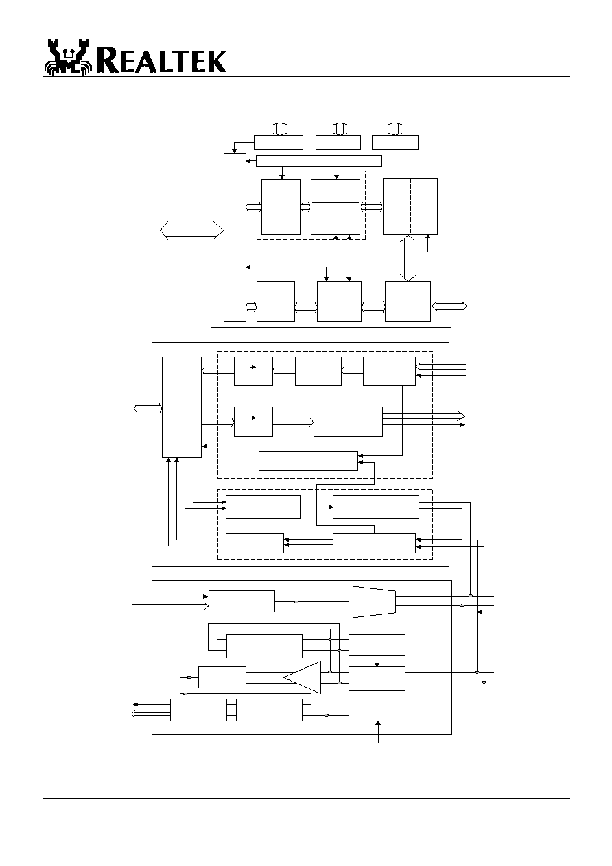
3. Block Diagram
MII
Interface
Interrupt
Control
Logic
FIFO
Transmit/
Receive
Logic
Interface
Early Interrupt
Control Logic
FIFO
Control
Logic
Packet Type
Discriminator
Power Control Logic
PCI Interface + Register
Packet Length
Register
Early Interrupt
Threshold
Register
Boot ROM
Interface
EEPROM
Interface
LED Driver
RXIN+
RXIN-
TXO+
TXO -
RXC 25M
25M
TXC 25M
TXD
RXD
TD+
Variable Current
3 Level
Driver
Master
PPL
Adaptive
Equalizer
Peak
Detect
3 Level
Comparator
Control
Voltage
MLT-3
to NRZI
Serial to
Parrallel
ck
data
Slave
PLL
Parrallel
to Serial
Baseline
wander
Correction
5B 4B
Decoder
Data
Alignment
Descrambler
4B 5B
Encoder
Scrambler
10/100
half/full
Switch
Logic
10/100M Auto-negotiation
Control Logic
Manchester coded
waveform
10M Output waveform
shaping
Data Recovery
Receive low pass filter
RXD
RXC 25M
TXD
TXC 25M
TXD10
TXC10
RXD10
RXC10
Link pulse
MII
Interface
10M
100M
PCI
Interface
MAC
PHY
Transceiver